
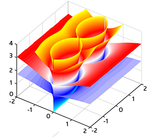
Plasmon energy states in an array of four graphene sheets. Each plane
represents different plasmon energy states resulting from different numbers of
electrons in each sheet.
A theoretical and numerical study of graphene sheets reveals a property
that may lead to novel opto-electric devices and circuits
One-atom-thick sheets of carbon —
known as graphene — have a range of electronic properties that scientists are
investigating for potential use in novel devices. Graphene’s optical properties
are also garnering attention, which may increase further as a result of
research from the A*STAR Institute of Materials Research and Engineering
(IMRE). Bing Wang of the IMRE and his co-workers have demonstrated that the
interactions of single graphene sheets in certain arrays allow efficient
control of light at the nanoscale1.
Light squeezed between single
graphene sheets can propagate more efficiently than along a single sheet. Wang
notes this could have important applications in optical-nanofocusing and in
superlens imaging of nanoscale objects. In conventional optical instruments,
light can be controlled only by structures that are about the same scale as its
wavelength, which for optical light is much greater than the thickness of
graphene. By utilizing surface plasmons, which are collective movements of
electrons at the surface of electrical conductors such as graphene, scientists
can focus light to the size of only a few nanometers.
Wang and his co-workers
calculated the theoretical propagation of surface plasmons in structures
consisting of single-atomic sheets of graphene, separated by an insulating
material. For small separations of around 20 nanometers, they found that the
surface plasmons in the graphene sheets interacted such that they became ‘coupled’
(see image). This theoretical coupling was very strong, unlike that found in
other materials, and greatly influenced the propagation of light between the
graphene sheets.
The researchers found, for
instance, that optical losses were reduced, so light could propagate for longer
distances. In addition, under a particular incoming angle for the light, the
study predicted that the refraction of the incoming beam would go in the
direction opposite to what is normally observed. Such an unusual negative refraction
can lead to remarkable effects such as superlensing, which allows imaging with
almost limitless resolution.
As graphene is a semiconductor
and not a metal, it offers many more possibilities than most other plasmonic
devices, comments the IMRE’s Jing Hua Teng, who led the research. “These
graphene sheet arrays may lead to dynamically controllable devices, thanks to
the easier tuning of graphene’s properties through external stimuli such as
electrical voltages.” Graphene also allows for an efficient coupling of the
plasmons to other objects nearby, such as molecules that are adsorbed on its
surface. Teng therefore says that the next step is to further explore the
interesting physics in graphene array structures and look into their immediate
applications.
The A*STAR-affiliated researchers
contributing to this research are from the Institute of Materials Research and
Engineering
VIDEO CAPTION:
The propagation of surface
plasmons. The plasmons move from the bottom of the screen to the top as a
function of the angle of incoming light.
References
- Wang, B., Zhang, X., García-Vidal, F. J., Yuan,
X. & Teng, J. Strong coupling of surface plasmon polaritons in
monolayer graphene sheet arrays. Physical Review Letters 109, 073901
(2012). | article
No comments:
Post a Comment